winnie jeng class notes

LC3 Registers

In order to supplement our understanding of LC3 datapath, we dive into Register File in finer details

The 8 LC3 General Purpose Registers live inside the Register File Circuit. They are small, fast memory with 16-bit addressability per register.

Figure 1 shows the Register File Circuit.
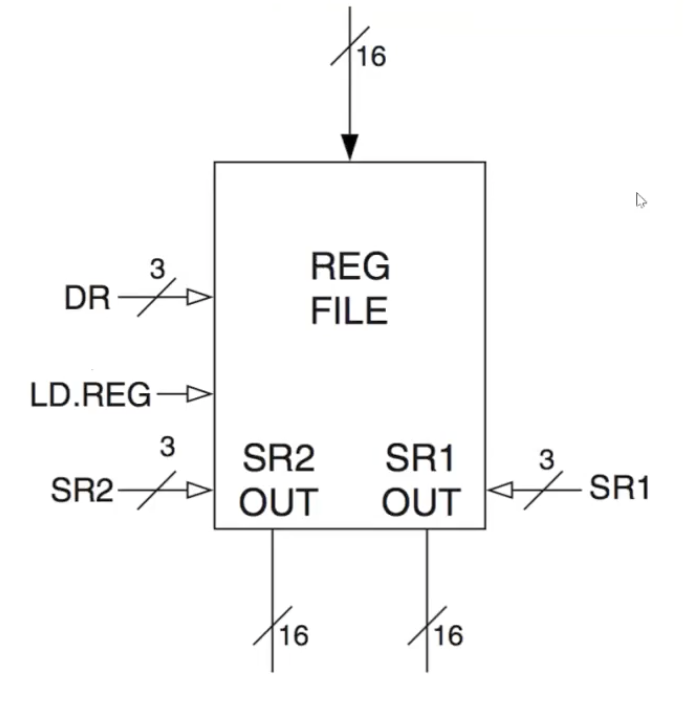
 LC3 Register

Input

  • The 16 wires going into the Reg File represents the input data that you want to save.
  • LD.REG is the 1-bit WE wire that remembers the data coming in.
  • DR stands for Destination Register; its 3-wire sends the location address of where to store the incoming data.
  • The Reg File is a dual-ported memory, which means that it can read 2 registers at a time–the SR1 (3-bit address) and SR2 (3-bit address).

  • SR1 stands for Source Register 1, which is the primary output that reads address number 0-7 from memory.
  • SR2 is the secondary output that reads a different address number 0-7 from memory.
  • Output

  • Whatever values are stored in the addresses that SR1 and SR2 read, they will each be outputed with the set of 16-bit wires

  • Recall an advantage of the Leader-Follower Flip Flop that is used to build registers–you can simultaneously read your next value as you write the current value. With LC3 File Reg, you can simulataneously read two register values as you write one register value in a single clock cycle.


    Supplementary lecture material: Dr. Caleb Southern, 06-03-2020

    Further reading: Introduction to Computing Systems: From Bits and Gates to C and Beyond, 3rd ed, Chapters 3.7