Combinational Logic Circuits
02 Jun 2020There are two fundamental kinds of logic structures–combinational and sequential. Combinational logic structures are decision elements that output based on the current inputs. Unlike the sequential logic circuits, they do not have information storage ability.
This post examines the three most common combinational logic circuits: decoder, mux, and adder. Adders can be further broken down to two types–full adder and half adder. Finally, we will see how programmable logic array (PLA) forms the foundational architecture whereupon we build our combinational logic device.
1) Decoder
A property of the decoder is that exactly one of its output is 1, and the rest of the outputs are 0’s.
A decoder with \(n\) inputs has \(2^n\) outputs.
Figure 1 shows a 3-bit decoder, and some variations of the inputs with respective output.

2) Mux
A multiplexer, commonly refered to as mux, is a switch that selects from \(2^n\) data inputs with \(n\) select lines, and propagate exactly \(1\) output. The \(2^n\) data input singals pass through a \(2^n\)-bit decoder and converge at an OR gate before being finally outputted.
Multiplexers economizes physical space by allowing multiple input sources to share a common selector channel.
Figure 2 shows a 4-to-1 mux with 2 selectors.

In this particular example, when the selector bits are 00, toggling the first input will turn on the output signal. When the selector bits are 01, toggling the first input will turn on the output signal. When the selector bits are 10, toggling the second input will turn on the output signal. When the selector bits are 01, toggling the third input will turn on the output signal, etc..
Ah, yes, order of the selector bits in Figure 2 is a bit wack, but no matter…you get the point. Just trace along the input wires to see toggling which data input with which selector bit-combination turns on the output.
3A) 1-Bit Adder (Full Adder)
A 1-bit Adder, also known as a full adder, takes in two 1-bit binary operands, consider for a possible carry-in operand, and perform binary addition.
Notice that a full adder is pretty much built with \(2^3 = 8\) decoders with two 4-input OR gates.
The output result of a full adder with three inputs–first operand, second operand, and carry-in–consists of a sum bit and a carry bit.
Figure 3 shows a truth table of the different input/output combination for a full adder.
| A | B | Cin | S | Cout | |
|---|---|---|---|---|---|
| 0 | 0 | 0 | 0 | 0 | |
| 0 | 0 | 1 | 1 | 0 | |
| 0 | 1 | 0 | 1 | 0 | |
| 0 | 1 | 1 | 0 | 1 | |
| 1 | 0 | 0 | 1 | 0 | |
| 1 | 0 | 1 | 0 | 1 | |
| 1 | 1 | 0 | 0 | 1 | |
| 1 | 1 | 1 | 1 | 1 |
Figure 4 shows the circuit design for a full adder and perform addition on some different configurations of the input bits.

3B) 4-Bit Adder
Much like the full adder, a 4-bit adder takes two operands and perform addition, while accounting for the carry-in and carry-out bits. However, more interesting than the 1-bit adder, each of the operand is 4 bits (surprise suprise).
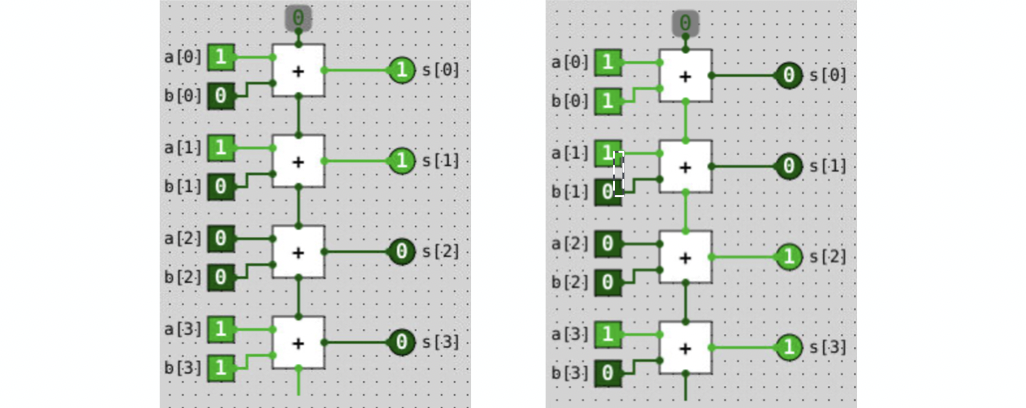
The structure of a 4-bit adder is very interesting–it’s chained by 3 full adder with 1 half-adder at the tail, which represents the most significant bit. The carry-out bit in the first three full adders becomes the carry-in bit in its next consecutive adder. Note that the last adder does not have a carry-out.
Figure 5 shows an example of a 4-bit adder with 2 examples.

In the first case of 1011(11) +0001(1), the first full-adder has a carry-out, which is propagated to the second adder as a carry-in. In the last adder (or the most significant adder if you will), there is no carry-in and no carry-out. Therefore, there is no overflow of the final output value 1100(13)
In the second case of 1011(11) +1000(8), the last adder has no carry-in but a carry-out. There is overflow of the final output value 0011(3) (!?!?)
But how do we know if we will encounter an overflow with our 4-bit adder? Well, how many numbers can you represent with 4 bits? \(2^4 = 16\) numbers! For unsigned integers, you can represent numbers 0 through 15.
So if you convert the binary operands from the second example into decimals, then you will be performing \(11 + 8 = 19\). Since 19 is clearly not in the range of 0 to 15, you know that it is an overflow.
4) The Programmable Logic Array (PLA)
The PLA is developed by Texas Instrument in 1970.
In its barest form, it is a set of programmable AND gates, followed by a set of programmable OR gates, followed by some buffers, on an integrated circuit plane.
The PLA can be reconfigured in many forms, and it is used in building not just combinational logic circuits, but also sequential logic units–that’s right! PLA is our bridge that links the two types of logical device into one integrated design.
Next, we will examine sequential logic units and storage elements.