Sequential Logic Circuits
03 Jun 2020
Sequential logic circuits have information storage ability–that is, sequential logic circuits can remember information of the previous states, which then affect the logic of the current and/or future states.
This feature of remembering the past state to make logical decision about the current or future states makes the circuits a finite state machine.
The storage elements of the finite state machine are called memories.
In this post, we will examine two basic sequential logic circuits–the R-S Latch and the Gated D Latch–and discuss how they are used to build registers, which are the storage elements in modern computer’s CPU.
Understanding these components would then lead us to exolore the concepts of address space and addressability.
R-S Latch
The R and S in R-S Latch stand for Reset and Set. R-S Latches are composed of two gates and two input. The R input is connected to one gate, and the S input is connected to the other gate. The output of each of the gate then serves as the second input for the other gate. Kind of a weird, twisted design, eh?
This weird, twisted design provides signal “feedback” that enables the cirucit to remember its previous logical state even if the controlling input signal changes.
The two logic gates of R-S Latch can either be both NAND Gates or both NOR Gates. Logics of the two different implementations for R-S Latch differ slightly, but are still very similar.
NAND R-S Latch
The NAND R-S Latch has 3 valid states:
Figure 1 shows the 3 valid + 1 invalid states of the NAND R-S Latch.

For inputs R = 0 and S = 1, the set bitis on so the current output is Q = 1 and the next output will be Qnext = 0.
For inputs R = 1 and S = 0, the reset bitis on so the current output is Q = 0 and the next output will be Qnext = 1.
For inputs R = 1 and S = 1, both the set bitand the reset bitare on. In such a case, outputs Q and Qnext hold whatever the current state is.
Inputs R = 0 and S = 0 are invalid for the NAND R-S Latch. If such inputs are set, circuit has high impedance and the current enters into a floating state.
Note that the outputs are always of opposite binary values.
Figure 2 provides a truth table for the NAND R-S Latch.
| R | S | Q | Qnext | |
|---|---|---|---|---|
| 0 | 0 | INV | INV | |
| 0 | 1 | 1 | 0 | |
| 1 | 0 | 0 | 1 | |
| 1 | 1 | HOLD | HOLD |
For the NOR R-S Latch, the logics for (R,S) = (0,0) and (R,S) = (1,1) are flipped.
Gated D Latch
The Gated D Latch is an improvement of the R-S Latch in that R-S Latch can set bit, reset bit, and even momentarily hold the current state. But what if we want to record the value that we are holding? Now this is much more similar to how actual memory works.
Gated D Latch has a record bit, also known as Write Enabled, or simply WE. If WE is set to 1, then it records the input and the output changes value to match the input value. When WE = 1, if data input = 0, then data output = 0, and if data input = 1, then data output = 1.
If WE is set to 0, then we ignore the data input and output remembers the last state of the data input. So if the last data input = 1 when WE = 1, now that WE = 0, regardless whether my current data input is 0 or 1, the data output holds the value 1.
[images here]
A Gated D latch is basically a 1 bit memory. But what if we want multiple-bit memory?
Registers
Registers are components that hold memory. The structure of a register is basically multiple Gated D Latches chained together in parallel.
A 4-Bit Register is basically four Gated D Latches chained together. We can store unsigned integers 0-15 in a 4-Bit Register.
Figure In this 4-Bit Register, the input bits are D0-3, and the output bits are Q0-3. There is one record input bit WE.
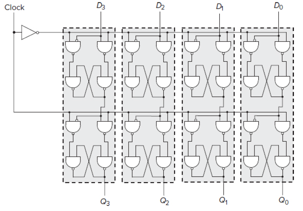
[Example image of 0110 with register]
Address and Addressability
Registers hold short-lived, but easily written/retrieved memories inside the CPU. Regular computer memories (RAM) are different than register memories. We are shifting gears a little to talk about computer memories.
Memories are only as good as if you can find them and access them. Without knowing the address of the memory, they’re useless.
Address space tells you the dimension of your memory array, e.g. arr[address-space]. A 4-bit register has an address space of \(2^4\) = 16, which means that it has 16 unique memory location.
Addressability tells you the memory of each memory location, e.g. int arr[] gives an array with addressability of the size of an integer, and char arr[] gives an array with addressability of the size of a character.
Memory
The basic building blocks of memory are 1) Decoder, 2) Multiplexers, and 3) Register (Gated D Latches).
Treating memory now as a black box, the input to memory are 1) address wires that describe the memory location, 2) a WE wire to record input, and 3) input data D. The output from memory is simply 1) output data Q.
Figure This memory has an address space of 2^2 = 4 (2 address wires) and an addressability of 8 (8 input wires).
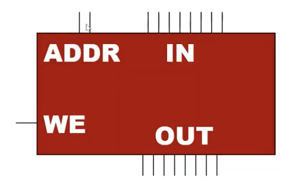
Figure shows a 4x3 memory. The dimension of a memory is address space x addressability. This memory shown has 4 addresses and 3 data input wires, which is actually quite uncommon to have an input of 3 wires–I don’t know any data type that represents 3 bits.
The two address wires pass through 4 decoders to determine the address space, and there are 12 Gated D Latches (the square components on the diagram ) connected to Muxes to select the bits to throw to the output. To store memory, turn the WE on, select the address to store the memory and select the desired data input. To read memory, turn the WE off, set the address bits, and read the data output from that memory address.
Every row is a memory address, and every column is the bit given to that memory address.
Clock
A clock is a square wave signal that oscillates between 0, ground, and 1 voltage. Sequential logic implies time, as we’re moving over time with states. Connecting the clock to WE helps us carry out sequential logic and step through the states.
Leader-Follower Flip Flop
A leader-follower flip flop is basically two Gated D Latches chained in series. The first latch has WE inverted in one of its input whereas the second Gated D Latch has WE passes through directly for one of its input.
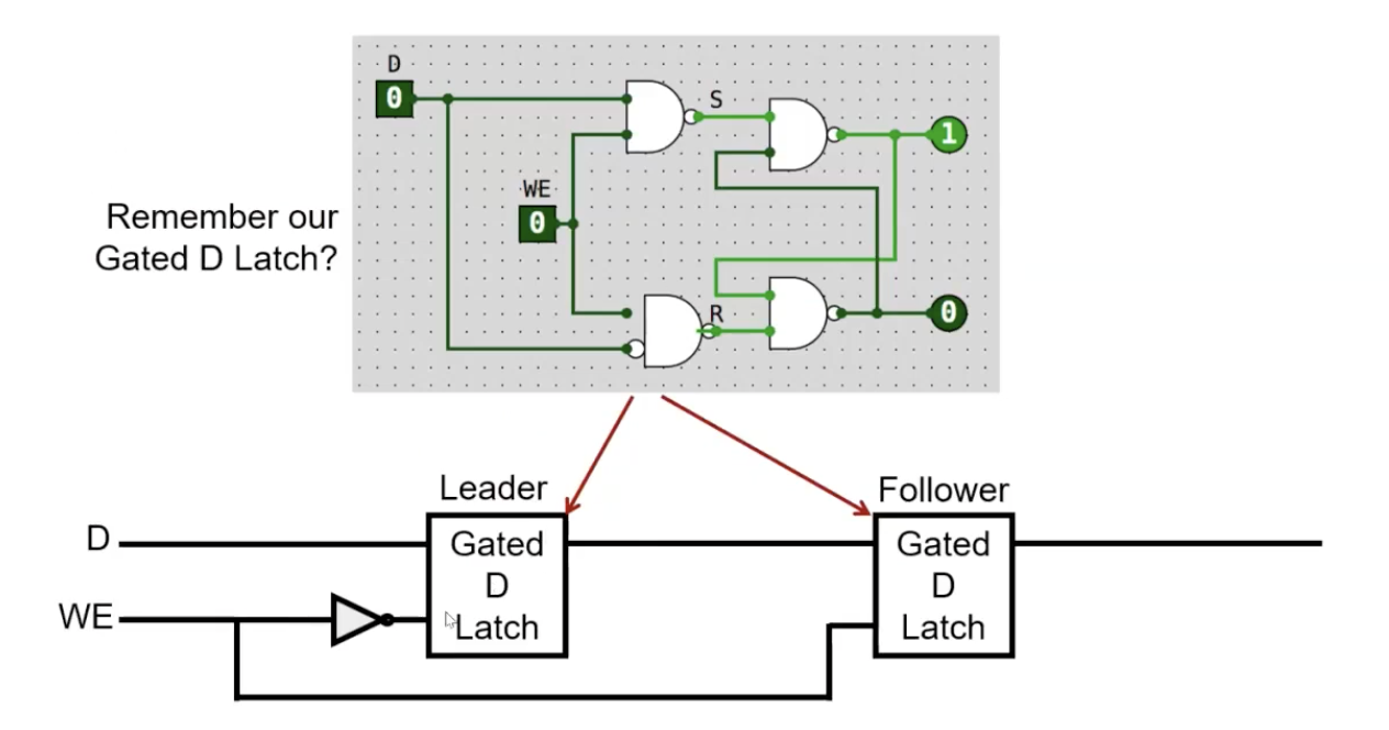
Connecting Clock to the Leader-Follower Flip Flop
When connecting a clock to a Leader-Follower flip flop, it controls operations like Adding to exactly once per clock cycle as the clock drives the WE. A Leader-Follower design allows you to record the next value to memory while outputting the current value.
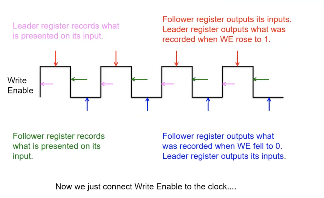
The Leader-Follower Flip Flop is also called a Register with edge-triggered setting (as opposed to a Register with level-triggered setting, where only WE and not the clock determines the output. A Level-triggered sequential circuit without a Leader-Follower design can yield unexpected result as the output of the device is used in computing the input of the same device. If the IO are not regulated by the clock cycle, speed of the transistors determines the timing of the cycle).
Figure shows a Leader-Follower Flip Flop connected to a clock.
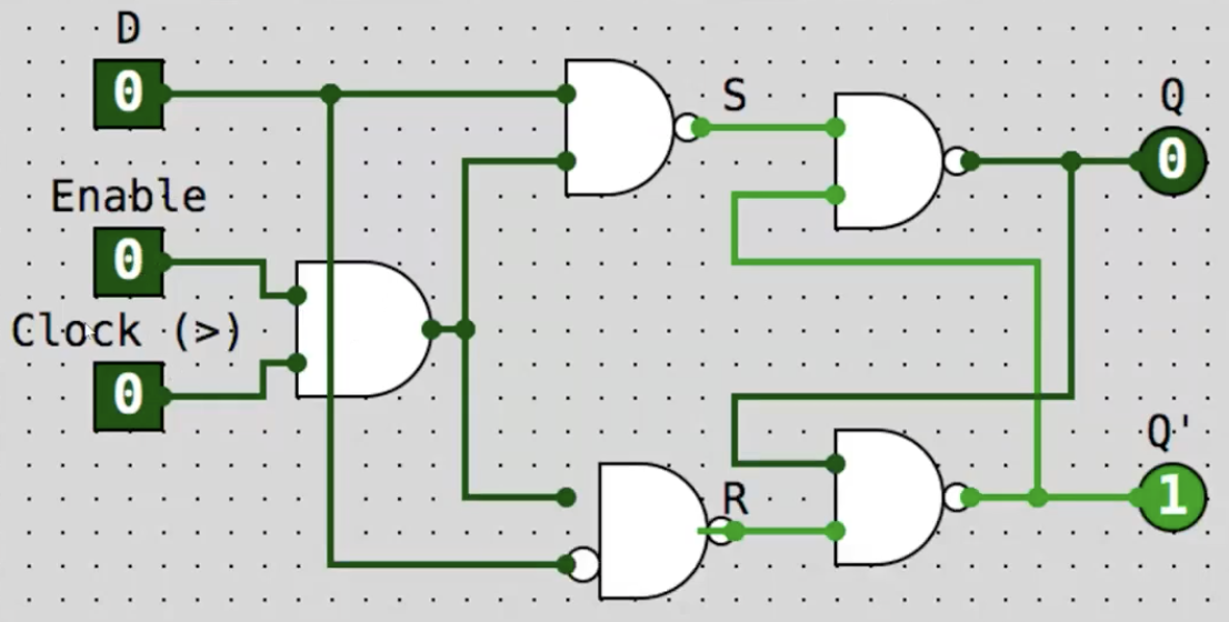
If we don’t want to output on every cycle, simply ANDthe WE with the clock signal–only when the clock and WE are both 1 will the flip flop writes.