LC3 Datapath
08 Jun 2020LC3 is a 16-bit processor introduced by Patt & Patel in the textbook Introduction to Computing System. We will be learning about computer architecture with LC3.
In LC3, there are 216 = 65536 unique memory addresses as address space. The addressability is 16 bits, which means that every single memory location contains a 16 bit value. Its architecture is the Von Neumann Model, and it has 8 general purpose registers and 16 bit instruciton size.
Note that since LC3 has 16 bits for addressability, it cannot do floating point representation easily, only integer operations, as floating points have 32 bits representation.
Figure 1 shows the datapath of LC3, which is just a large circuit diagram that shows how to build the logic components of the computer.

In the diagram, num/ represents the number of wires connected parallely to the component. For example, the arrow symbol with “2/” going into PCMUX indicates that there are 2 parallel selector bits/wires for the PCMUX.
Figure 2 shows the muxes of LC3. Muxes choose between two or more different inputs and produce one output.
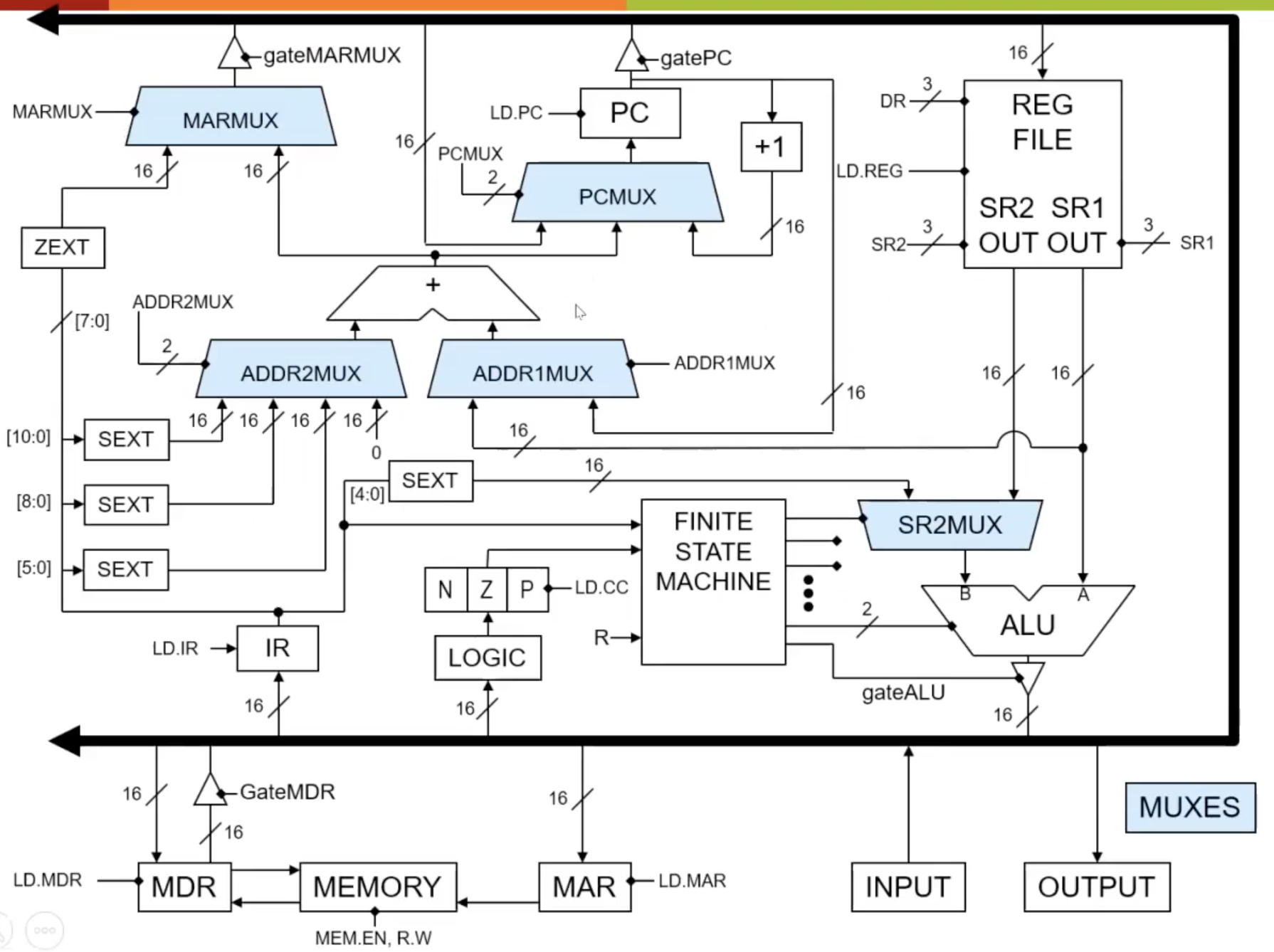
Figure 3 shows the states of LC3. States are set by registers, which is a form of memory.
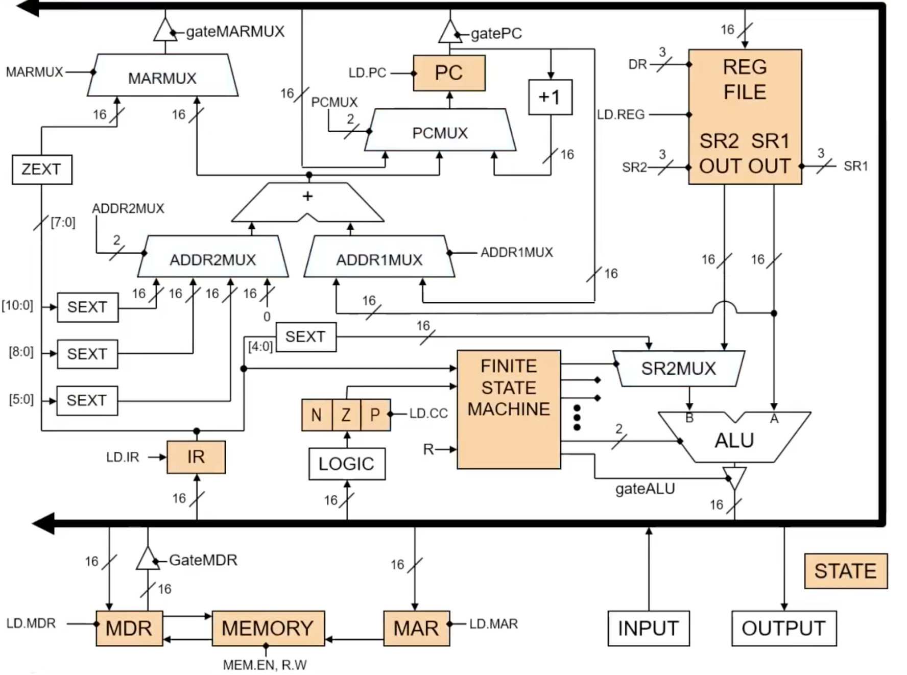
Figure 4 shows the computation components of LC3. They are made from combinational logic circuits
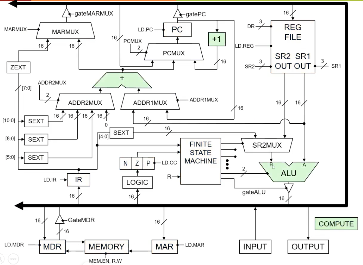
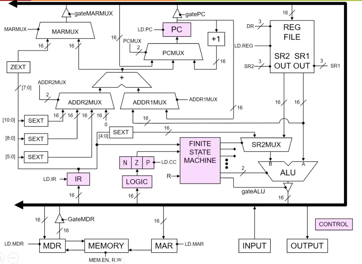
Figure 5 shows the control of LC3. Finite State Machine is the heart of the LC3 datapath, which controls the logic of the whole computer circuit step-by-step.
There is one more combinational logic circuit on the diagram which doesn’t belong to any part of the category–the Tri-State Buffer.
A regular Buffer, or Amplifier, is diagramattically expressed as a triangle gate without a bubble at the end (with the bubble, it becomes a NOTGate). Tri-State Buffer is a modified buffer with conditinoal logic to support the bus, which is simply 16 wires of the datapath that transport data from one component to the other with no transistors or logic.
Figure 6 shows an abstracted Tri-State Buffer and its controlled logic
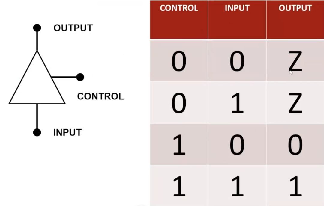 Figure 7 shows the implementation of a Tri-State Buffer
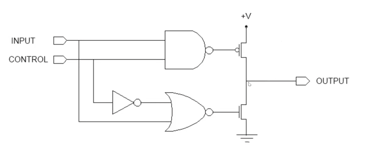
Tri-State Buffer allows the 16 wires of the bus to be shared amongst all the components along the datapath by selectively connecting and disconnecting input to be transported onto the bus; it does not allow more than one thing connected to the bus at any time, thereby preventing short circuit and datapath catching on fire.